

DSP(Double Side Polish)
Introduction & Applications in MEMS Processing
Double Side Polished (DSP) wafers provide ultra-high surface flatness and thickness uniformity, serving as a critical foundation for high-precision MEMS device manufacturing.
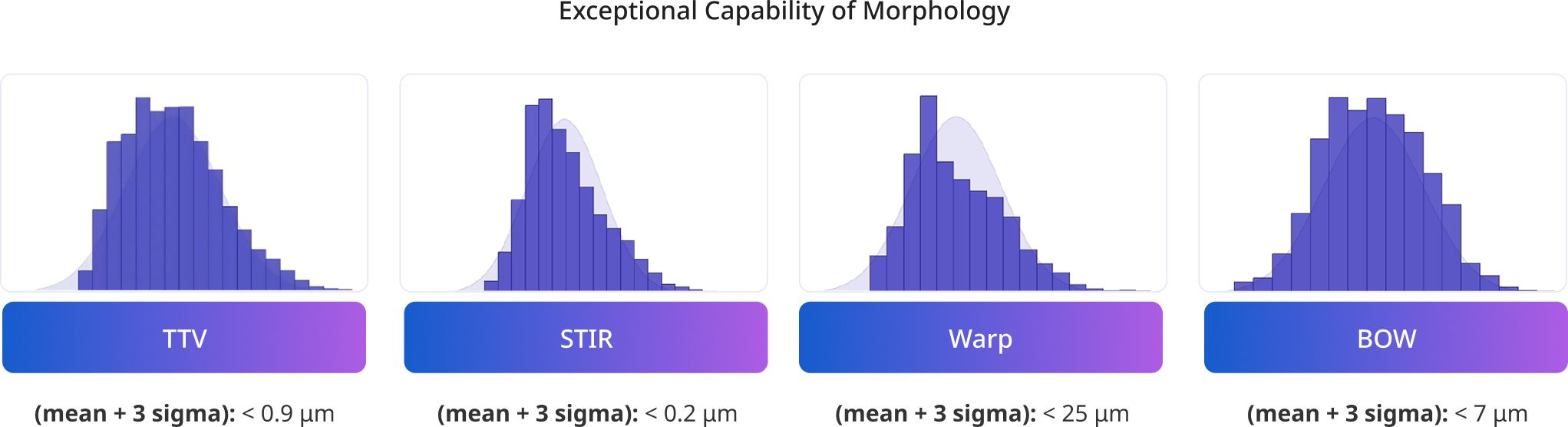
Precision double-side polishing significantly reduces surface roughness and thickness variation (TTV), ensuring uniformity across both the structural layer and the BOX layer to enhance mass-production yield and reliability.
Key Features
- High-Precision Double-Side Polishing
Delivers top and bottom surface flatness (TTV < 1 µm) and
Surface roughness < 1 nm RMS (customizable per spec) to minimize optical and mechanical interference. - Superior Thickness Uniformity
Uniform Device and BOX layer thickness, tailored for high-precision MEMS microstructures - Enhanced Yield & Reliability
Precise thickness control and planar surface minimize process defects, ideal for high-end MEMS mass production. - Multiple Wafer Size Support
Customizable for both 6-inch and 8-inch wafers.
Typical MEMS Applications
- MEMS Pressure Sensors
- MEMS Accelerometers / Gyroscopes
- MEMS Mirrors / Scanners
- Optical MEMS Devices (e.g., Microlenses, Actuated Optical Structures)
- Precision Mechanical MEMS Components (e.g., Micropumps, Microvalves)
DSP Wafer Advantages
- Precision double-side polishing ensures structural layer flatness and consistency for MEMS.
- High-yield design minimizes downstream processing defect risks.
- Supports versatile MEMS applications, from pressure sensors to optical MEMS.
- Customizable wafer sizes, layer thicknesses, and electrical parameters to meet R&D and volume production needs.
Please reach us at : [email protected]