

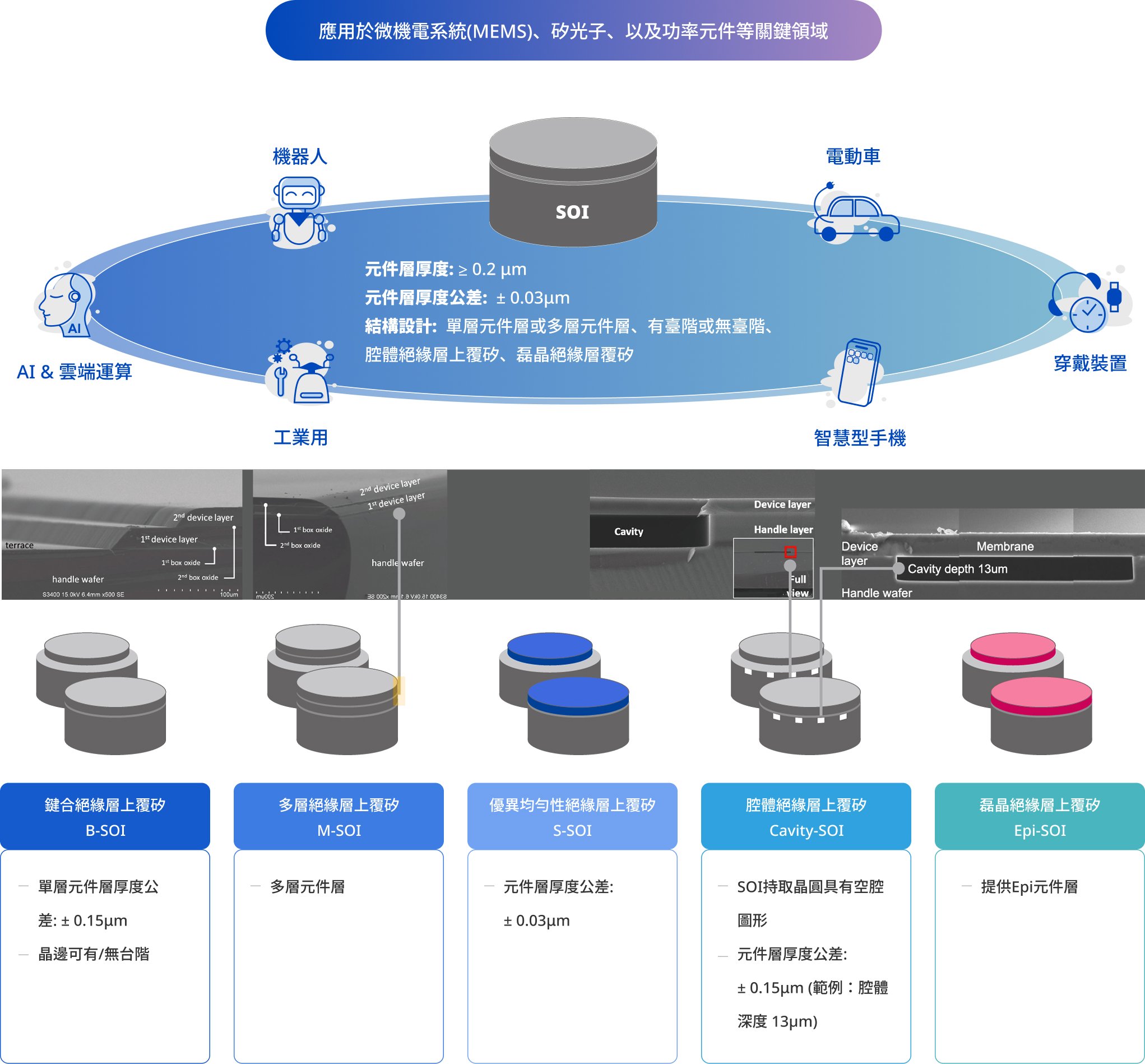
S-SOI (Superior-SOI)
In SOI wafer manufacturing, Device Layer thickness uniformity is the core metric determining semiconductor device performance, reliability, and volume production yield.
As next-generation high-precision MEMS and Silicon Photonics push thickness tolerances down to nanometer or sub-nanometer scales, conventional thinning and CMP technologies are reaching physical limits.
Against this backdrop, Ion Beam Trimming (IBT) has emerged as an ultra-precision surface modification technology essential for achieving extreme thickness uniformity in S-SOI substrates.
Typical Specifications (Customizable)
|
Parameter |
Specification |
|---|---|
|
Wafer Size |
6" / 8" (Evaluated per project) |
|
Device Layer Thickness |
± 0.45µm – 305µm |
|
BOX Thickness |
± 0.1 – 5µm |
|
Resistivity |
Specified per customer request |
|
Surface Roughness |
Meets advanced MEMS requirements |
Applications
- High-Precision MEMS & Sensors
- Silicon Photonics
- Ultra-Low Power, High-Performance Computing & IoT Devices
Please reach us at : [email protected]