

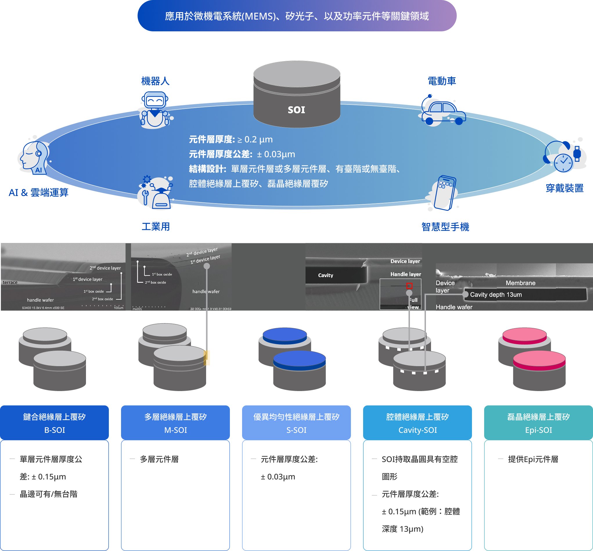
M-SOI(Multi-layers SOI)
Multi-Layer Device Layer SOI Wafers
M-SOI is not merely a single-layer Si/SiO₂ structure; it vertically stacks multiple Silicon Device Layers on a single wafer using precision processing, with each layer perfectly isolated by a buried oxide (BOX) layer.
Technical Advantages
1. Superior Isolation, Eliminating Interference
- Optimized Description: Physical isolation via multi-layer BOX minimizes parasitic capacitance and electrical crosstalk.
- Application Value: Essential for high-speed optical transceivers in AI data centers to ensure signal purity and reduce Bit Error Rate (BER).
2. High Integration: Reducing Footprint
- Optimized Description: Enables vertical 3D integration, stacking sensors, driver circuits, and processors together.
- Application Value: Meets Co-Packaged Optics (CPO) requirements to address rack space limitations.
3. Design Flexibility: Foundation for Heterogeneous Integration
- Optimized Description: Layer thickness, doping concentration, and crystal orientation can be independently customized for each silicon layer.
- Application Value: Allows using one layer for low-power logic and another layer for high-voltage MEMS actuation.
Typical Specifications (Customizable)
|
Parameter |
Specification |
|---|---|
|
Wafer Size |
6" / 8" (Evaluated per project) |
|
Device Layer Thickness |
± 0.45µm – 305µm |
|
BOX Thickness |
± 0.1 – 5µm |
|
Resistivity |
Specified per customer request |
|
Surface Roughness |
Meets advanced MEMS requirements |
Applications
MEMS Devices
- Pressure Sensors
- Accelerometers / Gyroscopes
- MEMS Mirrors
Please reach us at : [email protected]