
SOI


High-Precision SOI Wafers & Customized Process Solutions


Dedicated to High-Reliability Applications in MEMS, Power Semiconductors, and Silicon Photonics

From material design to process integration, SiliconWorks provides stable and volume-producible SOI/DSP wafer solutions to accelerate your time-to-market.


Core Advantages


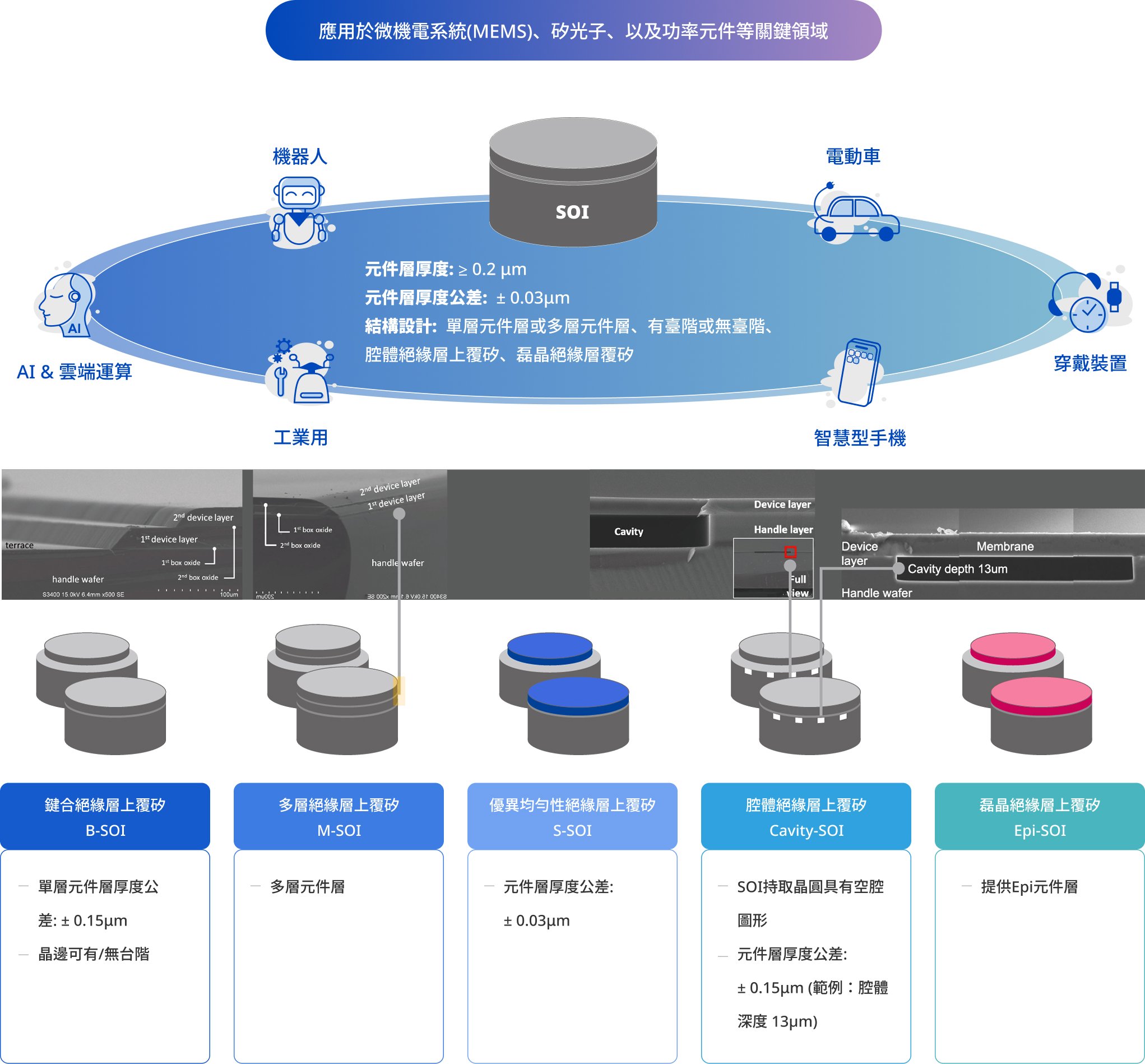
  • Diverse SOI / DSP Technology Platforms: B-SOI, M-SOI, Cavity-SOI, S-SOI, Epi-SOI, and DSP
  • High Customization Capability: Flexible adjustment for thickness, resistivity, BOX layer, and other parameters
  • Process Stability × High Consistency: Tailored for mass production and high-reliability requirements
  • Industry Expertise: Deeply rooted in MEMS and advanced semiconductor industries


soi pic


SOI Technology Comparison Overview


B-SOI vs Cavity-SOI vs Epi-SOI vs S-SOI


Parameter

B-SOI

Cavity-SOI

Epi-SOI

S-SOI

Fabrication Method

Wafer Bonding

Pre-etched Cavity + Bonding

Epitaxy + SOI Wafer Bonding

Wafer Bonding

Built-in Cavity

No

Yes (Built-in Cavity)

No

No

Layer Thickness Control

High

High

High

Ultra-High

Defect Density

Low

Low

Ultra-Low

Low

Process Complexity

Moderate

Low (Eliminates post-process etching/bonding)

Moderate to High

Moderate

Customization Flexibility

High

High (Structure-Oriented)

Ultra-High

High


How to Choose the Right SOI Technology?


  • Seeking proven volume production and broad compatibility → B-SOI
  • Requiring built-in cavities to simplify MEMS processing → Cavity-SOI
  • Prioritizing material quality, electrical, and optical performance → Epi-SOI
  • Requiring ultra-high thickness uniformity → S-SOI


B‑SOI(Bonded SOI)
High-Precision Bonded SOI Wafers

Designed for Mass Production of MEMS & Power Semiconductors


SiliconWorks B-SOI utilizes proven, volume-ready bonding processes, delivering stable layer thickness control, superior interface quality, and high consistency for all stages from R&D to mass production.


Key Features


  • High-Quality Wafer Bonding
    Ensures superior interface quality across Device Wafer, BOX, and Handle Wafer
  • Precise Layer Thickness Control
    Customizable Device Layer and BOX thickness based on application needs
  • High Yield × High Consistency
    Suitable for volume production of MEMS and power devices
  • Excellent Process Compatibility
    Seamless integration with mainstream MEMS and CMOS processes


Typical Specifications (Customizable)


Parameter

Specification

Wafer Size:

6" / 8" (Evaluated per project)

Device Layer Thickness

± 0.45µm – 305µm

BOX Thickness

± 0.1 – 5µm

Resistivity

Specified per customer request

Surface Roughness

Meets advanced MEMS requirements


Applications


MEMS Devices

  • Pressure Sensors
  • Accelerometers / Gyroscopes
  • MEMS Mirrors


Power Devices

  • Power ICs & Specialized Structural Components


Please reach us at : [email protected]

Co-Creating Sustainable Value, Driving Corporate Responsibility

Through energy efficiency, carbon reduction, transparent governance, and active community engagement, we shape a sustainable blueprint that balances semiconductor innovation with environmental stewardship.

Contact us