

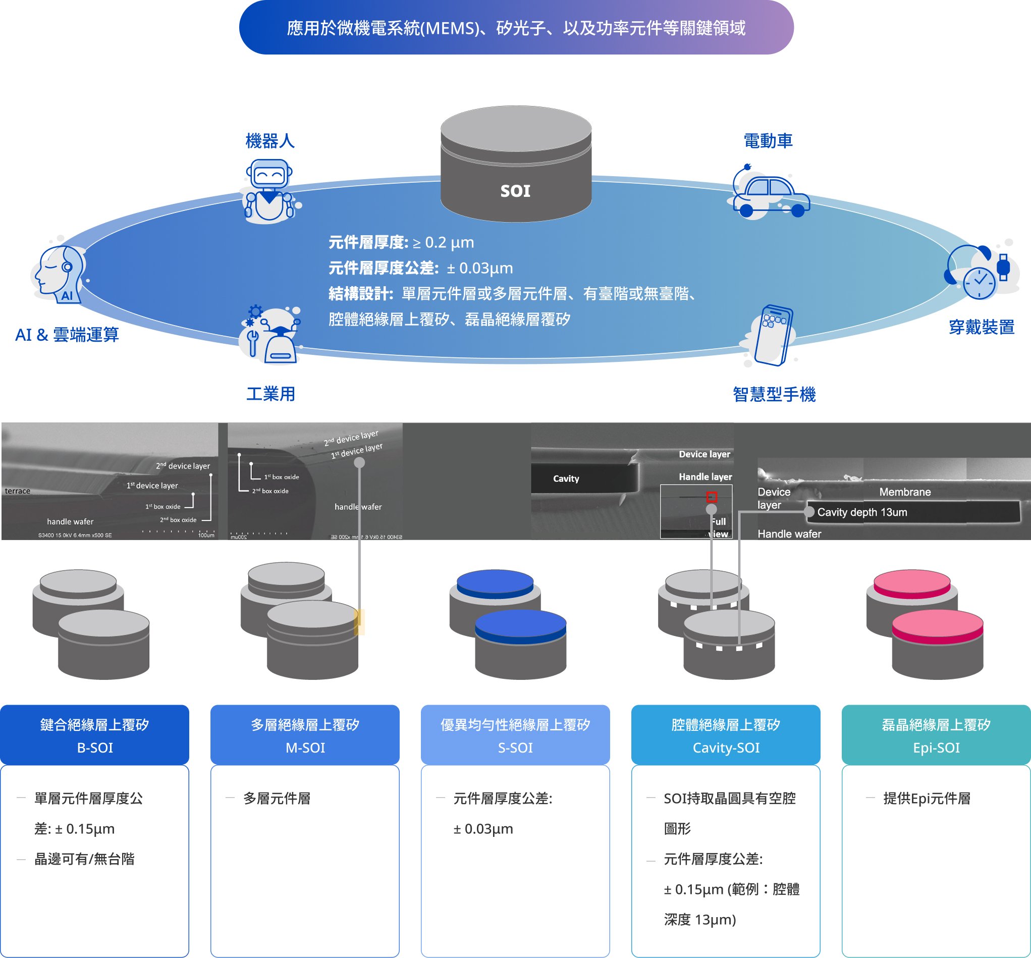
Epi-SOI(Epitaxial SOI)
High-Quality Epitaxial SOI Wafers
Engineered for Silicon Photonics, High-Speed Optoelectronics, & Advanced Device Architectures
SiliconWorks Epi-SOI combines high-quality epitaxial growth with SOI architecture, providing ultra-low defect density, exceptional thickness uniformity, and electrical control for high-sensitivity applications.
Key Features
- High-Quality Epitaxial Layer (Epitaxy)
Ultra-low defect density and crystal perfection for high-speed & optoelectronic applications - Precise Doping & Thickness Control
Supports customized resistivity and structural profile design - Superior Interface Quality
Reduces optical and electrical losses to enhance device performance - Advanced Process Compatibility
Ideal for Silicon Photonics, advanced CMOS, and heterogeneous integration
Typical Specifications (Customizable)
|
Parameter |
Specification |
|---|---|
|
Wafer Size |
6" / 8" (Evaluated per project) |
|
Epi Layer Thickness |
± 0.3 – 100µm |
|
BOX Thickness |
± 0.1 – 5µm |
|
Dopant Type |
N-type / P-type |
|
Resistivity |
Customized upon request |
Applications
- Silicon Photonics
- High-Speed Optoelectronic Devices
- Advanced Logic & Heterogeneous Integration
Please reach us at : [email protected]